Difference between revisions of "PCB (etching)"
From Electriki
Jump to navigationJump to search (New page: __NOEDITSECTION__ category:projects) |
|||
| Line 1: | Line 1: | ||
__NOEDITSECTION__ | __NOEDITSECTION__ | ||
[[category:projects]] | [[category:projects]] | ||
| + | <gallery widths=200px> | ||
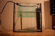
| + | Image:IMG 8646 before etching 1.JPG|The etching tank. | ||
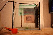
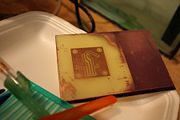
| + | Image:IMG 8649 before etching 2.JPG|Board treated with photoresistant laquer, UV light and developed later on. | ||
| + | Image:IMG 8652 the etching 3.JPG|Right after putting the board into etching tank (fresh acid). | ||
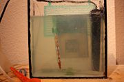
| + | Image:IMG 8656 the etching 4.JPG|Few minutes later... (the acid went a bit blue). | ||
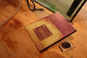
| + | Image:IMG 8658 after etching 5.JPG|Board right after taking it outta the bath. | ||
| + | Image:IMG 8660 after cleaning 6.JPG|Remaining laquer cleared up with acetone. | ||
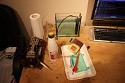
| + | Image:IMG 8662 whole set 7.JPG|The complete set of tools i used to etch this one. | ||
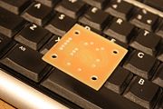
| + | Image:IMG 8664 board top 8.JPG|Top layer of board... (outta focus but CBA to fix it). | ||
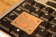
| + | Image:IMG 8666 board bottom 9.JPG|And the bottom layer. | ||
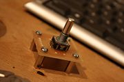
| + | Image:IMG 8668 assembled 10.JPG|Yeah i have soldered encoder already and screwed the distancers. | ||
| + | </gallery> | ||
