Difference between revisions of "PCB (etching)"
From Electriki
Jump to navigationJump to searchm |
|||
| (4 intermediate revisions by the same user not shown) | |||
| Line 1: | Line 1: | ||
__NOEDITSECTION__ | __NOEDITSECTION__ | ||
| − | [[category: | + | [[category:support]] |
<gallery widths=200px> | <gallery widths=200px> | ||
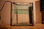
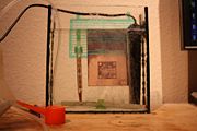
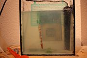
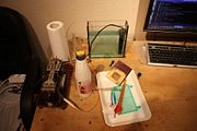
Image:IMG 8646 before etching 1.JPG|The etching tank. | Image:IMG 8646 before etching 1.JPG|The etching tank. | ||
| Line 11: | Line 11: | ||
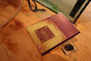
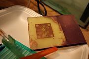
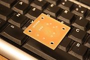
Image:IMG 8664 board top 8.JPG|Top layer of board... (outta focus but CBA to fix it). | Image:IMG 8664 board top 8.JPG|Top layer of board... (outta focus but CBA to fix it). | ||
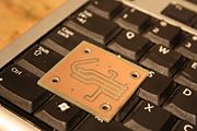
Image:IMG 8666 board bottom 9.JPG|And the bottom layer. | Image:IMG 8666 board bottom 9.JPG|And the bottom layer. | ||
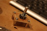
| − | Image:IMG 8668 assembled 10.JPG|Yeah i have soldered encoder already and screwed the | + | Image:IMG 8668 assembled 10.JPG|Yeah i have soldered encoder already and screwed the spacers. |
</gallery> | </gallery> | ||
| + | |||
| + | |||
| + | |||
| + | <gallery widths=200px> | ||
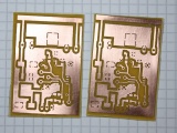
| + | Image:Tinning_IMG_2270.JPG|PCBs beforre tinning (copper layer exposed). | ||
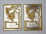
| + | Image:Tinning_IMG_2271.JPG|PCBs chemicaly tinned. | ||
| + | </gallery> | ||
| + | |||
| + | |||
| + | [[Category: Author_Pit]] | ||
Latest revision as of 22:56, 21 November 2011
