Difference between revisions of "PCB (etching)"
From Electriki
Jump to navigationJump to search| Line 12: | Line 12: | ||
Image:IMG 8666 board bottom 9.JPG|And the bottom layer. | Image:IMG 8666 board bottom 9.JPG|And the bottom layer. | ||
Image:IMG 8668 assembled 10.JPG|Yeah i have soldered encoder already and screwed the spacers. | Image:IMG 8668 assembled 10.JPG|Yeah i have soldered encoder already and screwed the spacers. | ||
| + | </gallery> | ||
| + | |||
| + | |||
| + | |||
| + | <gallery widths=200px> | ||
| + | Image:Tinning_IMG_2270.JPG|PCBs beforre tinning (copper layer exposed). | ||
| + | Image:Tinning_IMG_2271.JPG|PCBs chemicaly tinned. | ||
</gallery> | </gallery> | ||
Revision as of 10:42, 24 July 2011
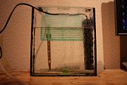
The etching tank.

Board treated with photoresistant laquer, UV light and developed later on.
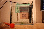
Right after putting the board into etching tank (fresh acid).
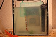
Few minutes later... (the acid went a bit blue).
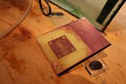
Board right after taking it outta the bath.
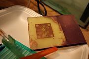
Remaining laquer cleared up with acetone.
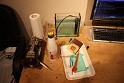
The complete set of tools i used to etch this one.
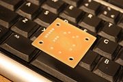
Top layer of board... (outta focus but CBA to fix it).
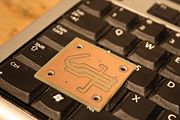
And the bottom layer.
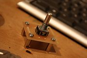
Yeah i have soldered encoder already and screwed the spacers.


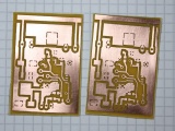
PCBs beforre tinning (copper layer exposed).
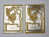
PCBs chemicaly tinned.

