Difference between revisions of "JTAG explorer toy"
| Line 100: | Line 100: | ||
* '''TDO''' (''Test Data out'') is used to shift bits out of the device. It changes on falling edge of <tt>TCK</tt>. | * '''TDO''' (''Test Data out'') is used to shift bits out of the device. It changes on falling edge of <tt>TCK</tt>. | ||
| − | See [[:Image:Michai_015_timing|Fig.5]] for an idea about timing of these signal. | + | See [[:Image:Michai_015_timing.jpg|Fig.5]] for an idea about timing of these signal. |
==== Daisy-chaining chips ==== | ==== Daisy-chaining chips ==== | ||
Revision as of 19:01, 4 January 2009
Contents
What is this, and, why..?
I heard a lot about JTAG, but never got to do anything with it, mainly because I CBA, and I didn't actually had to do anything with it.
This is of course bad, because...
JTAG is THE SHIT -- like Batman!
...or well, it's nice anyway.
Disclaimer
I interpreted the ATmega32-datasheet and (quite) some on-line docs as best as I could; however, if there's a bug/flaw somewhere, let me know please.
Note that this thing is totally useless, so questions/comments regarding will be ignored. Xmas season, too much time, so there :-)
Overview/summary
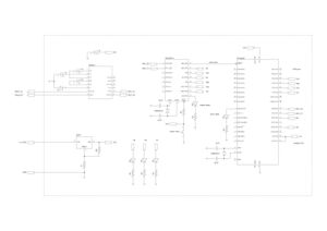
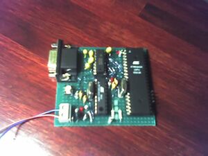
The idea for me was to make a simple toy-board with 2 MCU's on it -- one acting as JTAG host/master, and the other being JTAG-victim.
The PC talks to the master and slave through a serial protocol, to read/set pins, and so initiate JTAG-actions; master talks to slave only through its JTAG-port.
The master itself is not JTAG-enabled, but drives/reads the slave's JTAG-port I/O-pins.
What I would like to see
As I understood, JTAG offers a nice 'backdoor' into a (slave-)chip's state, and so that's what I would like to see; I'd like to...
- put it in, and take it out of reset (reset/suspend/resume)
- decouple core logic from I/O pins, and read/set them from boundary cells instead
- and some more, basically toy with it.
How JTAG works (as I understood it)
JTAG normally uses a single master/host to read/set states of one or more chips. There may be separate (JTAG) communication-channels between the host and each chip, or chips can be daisy-chained, so that the system's interface is kept simple and small.
Of course this is not complete; for more details, browse the lovely Internet.
Basic idea
Communication comes down to selecting which data to operate on, and then reading/ writing that data.
Single-chip setup
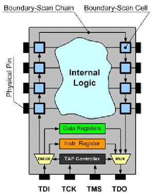
In a 1-chip JTAG-setup, the chip contains an instruction-register and a number of task-specific data-registers. The host can shift bits into each register; when a bit is shifted in, a bit falls out at the other end. Shifting always occurs in the same direction.
The host selects which data-register is active by entering an instruction-code, and then operates on the corresponding data-register. Writing/reading of both instruction- and data-registers occurs in the same way, by shifting bits in/out.
Multiple-chip setup
This works like above, except the complete system (more chips together) can be viewed as a number of big registers (where different parts/offsets in a register may live on different chips).
Bus-description
A chip offers access to its JTAG-subsystem through a TAP (Test Access Port), consisting of 4 (or 5) I/O-lines:
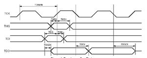
- TCK (Test ClocK) will be used to clock bits in/out of the device, and initiate mode-change.
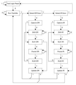
- TMS (Test Mode Select) is used to traverse through the TAP-controller's state-machine. It is sampled on rising edge of TCK.
- TDI (Test Data In) is used to shift bits into the device. It is sampled on rising edge of TCK.
- TDO (Test Data out) is used to shift bits out of the device. It changes on falling edge of TCK.
See Fig.5 for an idea about timing of these signal.
Daisy-chaining chips
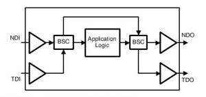
The TDI- and TDO-lines may be used to daisy-chain chips together -- chip #1's TDO is connected to chip #2's TDI. The host then shifts bits into chip #1's TDI, and catches bits falling out of the TDO of the last chip in the chain.
In such a daisy-chain, all chips share the TCK- and TMS-lines. Although sharing a clock may be normal, the common TMS-line was quite surprising to yours truly. But it still makes sense!
work in progress, tumdedum...

