Difference between revisions of "JTAG explorer toy"
| Line 52: | Line 52: | ||
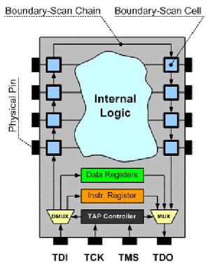
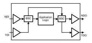
* decouple core logic from I/O pins, and read/set them from [[:Image:Michai_015_bsc.jpg|boundary cells]] instead | * decouple core logic from I/O pins, and read/set them from [[:Image:Michai_015_bsc.jpg|boundary cells]] instead | ||
* and some more, basically '''toy with it'''. | * and some more, basically '''toy with it'''. | ||
| + | |||
| + | == JTAG basics (as I understood it) == | ||
| + | |||
| + | JTAG normally uses a single master/host to read/set states of one or more chips. | ||
| + | There may be separate (JTAG) communication-channels between the host and each chip, | ||
| + | or chips can be daisy-chained, so that the system's interface is kept simple and | ||
| + | small. | ||
| + | |||
| + | === Bus-description === | ||
| + | |||
| + | A chip offers access to its JTAG-subsystem through a TAP (''Test Access Port''), | ||
| + | consisting of 4 (or 5) I/O-lines: | ||
| + | * '''TCK''' (''Test ClocK'') will be used to clock bits in/out of the device, and initiate mode-change. | ||
| + | * '''TMS''' (''Test Mode Select'') is used to traverse through the TAP-controller's state-machine. It is sampled on rising edge of <tt>TCK</tt>. | ||
| + | * '''TDI''' (''Test Data In'') is used to shift bits into the device. It is sampled on rising edge of <tt>TCK</tt>. | ||
| + | * '''TDO''' (''Test Data out'') is used to shift bits out of the device. It changes on falling edge of <tt>TCK</tt>. | ||
| + | |||
| + | ==== Daisy-chaining chips ==== | ||
| + | |||
| + | The <tt>TDI</tt>- and <tt>TDO</tt>-lines may be used to daisy-chain chips together -- | ||
| + | chip #1's <tt>TDO</tt> is connected to chip #2's <tt>TDI</tt>. The host then shifts | ||
| + | bits into chip #1's <tt>TDI</tt>, and catches bits falling out of the <tt>TDO</tt> of | ||
| + | the last chip in the chain. | ||
| + | |||
| + | In such a daisy-chain, all chips share the <tt>TCK</tt>- and <tt>TMS</tt>-lines. | ||
| + | Although sharing a clock, the common <tt>TMS</tt>-line was quite surprising to | ||
| + | yours truly. But it still makes sense! | ||
---- | ---- | ||
work in progress, tumdedum... | work in progress, tumdedum... | ||
Revision as of 18:25, 4 January 2009
Contents
What is this, and, why..?
I heard a lot about JTAG, but never got to do anything with it, mainly because I CBA, and I didn't actually had to do anything with it.
This is of course bad, because...
JTAG is THE SHIT -- like Batman!
...or well, it's nice anyway.
Disclaimer
I interpreted the ATmega32-datasheet and (quite) some on-line docs as best as I could; however, if there's a bug/flaw somewhere, let me know please.
Note that this thing is totally useless, so questions/comments regarding will be ignored. Xmas season, too much time, so there :-)
Overview/summary
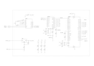
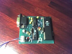
The idea for me was to make a simple toy-board with 2 MCU's on it -- one acting as JTAG host/master, and the other being JTAG-victim.
The PC talks to the master and slave through a serial protocol, to read/set pins, and so initiate JTAG-actions; master talks to slave only through its JTAG-port.
The master itself is not JTAG-enabled, but drives/reads the slave's JTAG-port I/O-pins.
What I would like to see
As I understood, JTAG offers a nice 'backdoor' into a (slave-)chip's state, and so that's what I would like to see; I'd like to...
- put it in, and take it out of reset (reset/suspend/resume)
- decouple core logic from I/O pins, and read/set them from boundary cells instead
- and some more, basically toy with it.
JTAG basics (as I understood it)
JTAG normally uses a single master/host to read/set states of one or more chips. There may be separate (JTAG) communication-channels between the host and each chip, or chips can be daisy-chained, so that the system's interface is kept simple and small.
Bus-description
A chip offers access to its JTAG-subsystem through a TAP (Test Access Port), consisting of 4 (or 5) I/O-lines:
- TCK (Test ClocK) will be used to clock bits in/out of the device, and initiate mode-change.
- TMS (Test Mode Select) is used to traverse through the TAP-controller's state-machine. It is sampled on rising edge of TCK.
- TDI (Test Data In) is used to shift bits into the device. It is sampled on rising edge of TCK.
- TDO (Test Data out) is used to shift bits out of the device. It changes on falling edge of TCK.
Daisy-chaining chips
The TDI- and TDO-lines may be used to daisy-chain chips together -- chip #1's TDO is connected to chip #2's TDI. The host then shifts bits into chip #1's TDI, and catches bits falling out of the TDO of the last chip in the chain.
In such a daisy-chain, all chips share the TCK- and TMS-lines. Although sharing a clock, the common TMS-line was quite surprising to yours truly. But it still makes sense!
work in progress, tumdedum...

