Difference between revisions of "Dual channel El Cheapo pulse generator"
| Line 4: | Line 4: | ||
== So, what is this all about? == | == So, what is this all about? == | ||
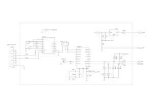
| − | [[Image:Michai_013_all.jpg|thumb|'''Fig.1: | + | [[Image:Michai_013_all.jpg|thumb|'''Fig.1: schematic.''' An ATtiny2313 receives a constant bitstream from a host-PC, and outputs the next bit/sample on each of 2 output-channels at fixed intervals.]] |
| + | |||
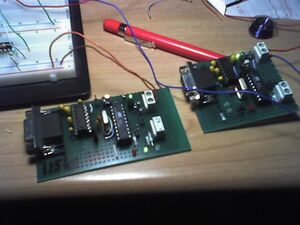
| + | [[Image:Michai_013_old_and_new_board.jpg|thumb|\\\Fig.2: old and new board.''' New one (left) still lacked clamp-diodes and series-resistors at time of pic-taking, mainly because of CBA.]] | ||
For some thing at work it was useful/necessary to generate a ''not-too-tast'', ''not-too-perfect'' yet arbitrary long and complex 2-channel digital signal. The thing described here is not that interesting, but can be built in a jiffy (2.5 hours by yours truly, starting from scratch :-) and is really cheap. | For some thing at work it was useful/necessary to generate a ''not-too-tast'', ''not-too-perfect'' yet arbitrary long and complex 2-channel digital signal. The thing described here is not that interesting, but can be built in a jiffy (2.5 hours by yours truly, starting from scratch :-) and is really cheap. | ||
| Line 16: | Line 18: | ||
=== Workhorse === | === Workhorse === | ||
| − | Workhorse (although it's burning cycles most of the time) is the faithful ATtiny2313 (although the [[:Image:Michai_013_all.jpg|schematic]] | + | Workhorse (although it's burning cycles most of the time) is the faithful ATtiny2313 (although the [[:Image:Michai_013_all.jpg|schematic in fig.1]] shows an AT90s2313 there). Input-bitstream comes from a RS232 connection from a host-PC, although a 'self-test' jumper can be closed to have it feed a nice bitstream to itself - mainly useful to test output-levels and -timing. Samples are output as 0V (low) or 5V (high) on 2 pins 'A' and 'B'. |
=== Safety-stuff === | === Safety-stuff === | ||
| − | This is the 3rd or even 4th unit I had the honour of soldering together; the other ones blew up, quite literally. Looking at | + | This is the 3rd or even 4th unit I had the honour of soldering together; the other ones blew up, quite literally. Looking at [[:Image:Michai_013_all.jpg|fig.1]], a diode after the 24VDC-terminal can be seen, as well as 2 clamp-diodes for each channel. In addition, a 4k7 resistor is placed after the clamp-diodes. This prevents damage in case of short-circuit or connecting an output to the gnd- or 24V-rail. |
== Software == | == Software == | ||
| Line 76: | Line 78: | ||
== So... what does it look like? == | == So... what does it look like? == | ||
| − | Well, | + | Well, see [[:Image:Michai_013_old_and_new_board.jpg|fig.2]] for an idea. 24VDC, gnd and both channels A and B can be connected using screw-terminals. Serial DE-9 is glued onto the board using superglue. The underside (not shown here) is just solder and copper; best kept on a non-conducting desk ;-) |
== Drawbacks == | == Drawbacks == | ||
Revision as of 21:32, 30 December 2008
Contents
So, what is this all about?
For some thing at work it was useful/necessary to generate a not-too-tast, not-too-perfect yet arbitrary long and complex 2-channel digital signal. The thing described here is not that interesting, but can be built in a jiffy (2.5 hours by yours truly, starting from scratch :-) and is really cheap.
The device itself acts as a dumb interpreter/timer of an incoming headerless bitstream (2 bits per sample, ad inifinitum), and outputs samples on each of 2 output-channels (A and B) at fixed intervals.
Hardware
Apart from a fairly uninteresting LM317 regulator and an equally boring Maxim MAX232 level-converter, there is...
Workhorse
Workhorse (although it's burning cycles most of the time) is the faithful ATtiny2313 (although the schematic in fig.1 shows an AT90s2313 there). Input-bitstream comes from a RS232 connection from a host-PC, although a 'self-test' jumper can be closed to have it feed a nice bitstream to itself - mainly useful to test output-levels and -timing. Samples are output as 0V (low) or 5V (high) on 2 pins 'A' and 'B'.
Safety-stuff
This is the 3rd or even 4th unit I had the honour of soldering together; the other ones blew up, quite literally. Looking at fig.1, a diode after the 24VDC-terminal can be seen, as well as 2 clamp-diodes for each channel. In addition, a 4k7 resistor is placed after the clamp-diodes. This prevents damage in case of short-circuit or connecting an output to the gnd- or 24V-rail.
Software
This is the less-boring part, perhaps. Software consists of a real-time part (inside the MCU) and a piece of software on PC that basically feeds the device with a bitstream. The latter can be your average TeraTerm.EXE, or it can be a custom interpreter/generator - I chose the latter.
MCU-software
The bitstream from the PC arrives in an 10-bit frame (startbit + 8N1) @ 115k2. Only 8 useful bits are present in each frame. Since a sample-(pair) consists of 2 bits (1 for each channel, to be output simultaneously), this gives us a sample-rate of ( 115200 / 10 ) * 4 ) ~ 46 kHz = freq_sample. This is not just a Good Idea - it's a fact of life, and follows directly from sample-size (2 bits), frame-layout (10 bits) and serial bit-time ( 1 / 115200 ). We can only output samples at freq_sample Hz using this simple 'bitstream'-method, period.
Therefore, 1 sample-period = ( 1 / freq_sample ) ~ 21.7 usec. Bytes will be arriving (assuming there is no delay between serial frames, i.o.w. each stop-bit is immediately followed by the start-bit for the next frame) at ( (1 / 115200 ) * 10 ) ~ 86.8 usec = ( 1 / freq_frame ). This makes sense, since freq_sample = ( 4 * freq_frame ), since there are 4 samples in a frame. Lovely.
The software will basically do the following:
wait for a byte, then, 4 times in a row, snoop the next 2 sample-bits from the byte at freq_sample. After that, the cycle repeats when a new byte comes in.
To do this, 2 interrupts -'Rx-complete' and a timer - are used. The timer interrupt is normally disabled, but when enabled, is executed when a user-writable, but automatically incrementing timer-register tmr_count overflows/wraps.
Pseudo-code for the RXC-handler:
RXC_ISR()
{
  sample_byte = receive_from_serial();
  num_remaining_sample = 4;
  tmr = T_first;
  enable_timer_interrupt();
}
Pseudo-code for the timer-handler:
TMR_ISR()
{
  bit_for_chan_A = sample_byte & 1;
  bit_for_chan_B = !!( sample_byte & 1 );
  output_dual_channel_sample( bit_for_chan_A, bit_for_chan_B );
  if ( --num_remaining_sample ) {
    tmr = T_next_sample;
  }
  else {
    disable_timer_interrupt();
  }
}
An that's basically all. Meanwhile, the main()-routine is keeping itself busy by stuffing 0x78-bytes our of its serial port (which give a fairly interesting gray'ish pattern when viewed on a scope). When aforementioned jumper is set to test-mode, this pattern will be output on channels A and B.
PC-software (interpreter/generator)
>>>bleep.<<<
So... what does it look like?
Well, see fig.2 for an idea. 24VDC, gnd and both channels A and B can be connected using screw-terminals. Serial DE-9 is glued onto the board using superglue. The underside (not shown here) is just solder and copper; best kept on a non-conducting desk ;-)
Drawbacks
2 things that are sub-optimal perhaps are...
- samples are output at discrete intervals (46 kHz); i.e. it's impossible to make a clean 40 kHz pattern
- there should not be gaps in between serial frames. A good old 16550A with a 4k Tx-buffer on a non-ancient PC should have no problems with this; however, I seen USB-to-serial converters screw this up on 2 occasions. Depending on the application this might or might not be a problem.
Have fun -- Michai

