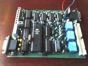
Flow-X IO interface board
Contents
So what is this anyway?
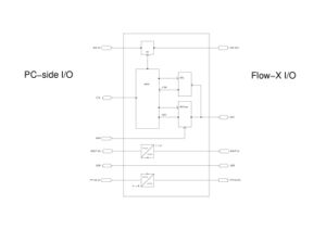
Below follows a description of a nice hobby-project to make an interface board that basically sits between a PC and an I/O module, to read module-outputs and stimulate module-inputs See Fig.0 for an idea. Schematics are done using gEDA's gschem, should you wonder.
Flow-X module
This is a small but very nice modular flowcomputer for the oil- and gas-industry; since I toy with/at this thing at work, why not make a little something to make Life a bit Nicer.
Interface-board
It would be nice to test test and provide stimuli for various digital/analog I/O's on the module from a PC, while meanwhile trying to keep it safe, or rather fool-proof in case I/O is misconfigured (i.e. misconfigured 'low' output connected to 'high' output), because we all make mistakes.
Some of the module's I/O is read/stimulated by the interface-board directly, while for other signals, the board only multiplexes signals or even simply passes them through to a host-PC. All I/O the board is capable of reading/stimulating itself, is passed to/from a host-PC using a serial protocol. Remaining I/O to be read/stimulated is psysically connected to the board, where it is multiplexed or just passed through to the module.
Covered I/O
Each interface-board only covers half of the module's I/O; therefore, 2 boards are needed to read/stimulate all I/O on a single module. Each board covers the following module-I/O:
1 RS-232/RS-422/RS-485 serial port
Simply passed through from module to host-PC; interface-board only provides a DE-9 connector for convenience sake.
1 PT100 resistance temperature measurement input
Resistance (or temperature) for the module can be specified by supplying an external voltage (0..5V) to the board. The signal is buffered by an opamp and then used to drive a high-intensity LED glued to a LDR. Current is limited to 27mA, just because we are very nice. In fact 27mA is insanely high come to think of it.
3 analog inputs, configurable for current/voltage
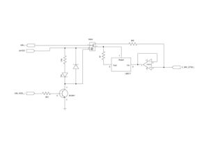
In case of current-input, the module basically reads the voltage over an internal shunt-resistor. This current can be controlled by feeding the board with a voltage (0..5V), which is buffered by an opamp and fed into the shunt. Current is again limited to 27mA; this is low enough as to not cause damage in the module. V/I will not be linear, mainly because of the current-limiter (LM317), but this can be compensated by software. See Fig.1 for the general idea.
In case of voltage input, the board simply places a safety-resistor in between the voltage (0..5V) offered to the board and the module. A relais on the board switches between current/voltage modes.
2 analog current-outputs
To read outputs from these 4..20mA outputs, the board simply contains a 220ohm shunt for each, and outputs the voltage over each shunt as output-level. Software will do conversion back to current.
8 open-collector digital I/O pins
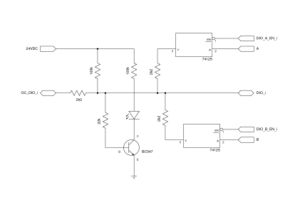
Because the module only has open-collector I/O's, the board provides a 'weak' 4.5V using a voltage-divider. For each digital channel, the module-side can be either input or output. The board-side can be input and output as well; damage because of misconfiguration is eliminated by a series-resistor (see Fig.2).
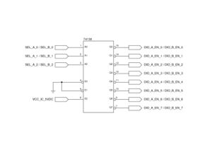
In addition to reading and stimulating the module's digital I/O, 2 auxiliary signals supplied to the board ('A' and 'B') may each be assigned to a digital I/O using a decoder and tristate buffers. Misconfiguration will not lead to damage by using series-resistors.
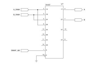
Auxiliary input 'A' can be assigned to module-inputs 0..6, while 'B' can be assigned to module-inputs 1..7. Signals 'A' and 'B can be 'parked' (decoupled) by assigning them to pins 7 and 0, respectively. To allow for any arbitrary assignment of 'A' and 'B', a swap-function is implemented in the board. See Fig.3 for the decoding/assignment, and Fig.4 for swapping A/B using a multiplexer.
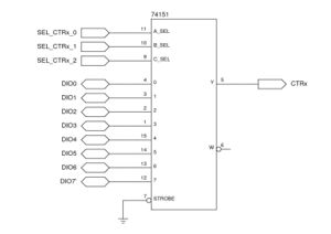
The microcontroller on the interface-board also has 2 counters; each counter can be assigned to any digital channel (0..7). Counters can be disabled/enabled and configured for positive or negative logic separately. Counters are passive, and don't influence I/O lines in any way. See Fig.5 for multiplexing the 8 DIO-lines to 1 counter-input.
Microcontroller and software
Of course there is a MCU in here! The mighty (in size) ATmega32 (DIP-40) manages all digital I/O, multiplexing and selection of signals. It runs on a 7.3728 MHz crystal, and communicates to a host-PC over a serial link @ 115k2 bps.
Software functionality
MCU-software roughly implements the following functionality:
- set direction and value of DIO-pins DIO0..7
- read status of DIO-pins configured as input
- configure individual counters CTR0 and CTR1 to count on rising/falling edge, reset counter, read counter-value
- assign aux inputs A and B to DIO-pins DIO0..7, swap or decouple them
- select analog mode (current/voltage) for each 3 of the module's analog input channels
- selftest-mode, without need for host-PC
These are all implemented fairly easy, and mostly map 1:1 to basic MCU features. In fact, the only 'feature' used is the external-event counter for CTR0 and CTR1.
Pin assignments
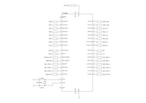
As can be seen in Fig.6, I/O-pins are given the following functions:
- general purpose digital I/O DIO0..7 (8 pins)
- CTR0 and CTR1 inputs (2 pins)
- status-LED output (1 pin)
- swap aux inputs A/B enable (1 pin)
- CTR0 and CTR1 DIO-pin assignment select (3 pins for each counter, 6 in total)
- aux input A/B DIO-pin assignment (3 pins for each input, 6 in total)
- voltage-mode enable for each of the module's analog input (3 pins)
- status-LEDs for CTR0 and CTR1 (not sure what to do with those; 2 pins)
Basically, it reads/sets I/O pins and thus only handles digital I/O. Analog I/O is handled completely separate from the MCU. Apart from all these plus reset and serial Tx/Rx, there was 1 pin left, so why not make that a 'selftest' input using a pullup and a jumper.
Board/host-PC protocol
The host-PC talks to the software in the MCU using a simple ASCII-based, human-readable command-set. Each command is terminated by CRLF. If the command was a value-request, the MCU answers with the value; finally, the MCU sends a status-code (2-digit hex code) indicating status of last command. This allows for testing using terminal emulator, and avoids timing problems from sending commands too fast; host-PC should wait for status-reply before sending next command.
Commands may take a number of arguments; each argument is given using a 2-digit hex notation. There is no separator between the command-identifier and arguments, or between arguments.
The protocol is described here (parameters shown using '<'...'>' markers):
| command: | reply: | descr: |
| dr | port-value (2-digit hex) | read value of DIO-port |
| dw<setmask><value> | - | write to DIO-port; only pins masked in 'setmask' that are configured as output-pins are written according to 'value' |
| dd<setmask><direction_mask> | - | set direction of DIO-pins; only pins masked in 'setmask' are written according to 'direction_mask' (0=input, 1=output) |
| ce<counter_index><edge_rising> | - | edge-select for counter 'counter_index'; 0=falling, nonzero=rising |
| cr<counter_index> | counter-value (32 bit unsigned hex) | read current value of counter; it is safe to do so while counter is active/busy |
| cc<counter_index> | - | clear value of counter 'counter_index' |
| cs<counter_index><DIO_pin_index> | - | select DIO-pin 'DIO_pin_index' as input for counter 'counter_index' |
| es<DIO_pin_index_A><DIO_pin_index_B> | - | select aux channels A and B as inputs for DIO-pins, or disconnect them (use 'ff' as index); swap pins if necessary |
| as<AIn_index><enable_voltage> | - | select AIn-channel 'AIn_index' for voltage or current (0=current, nonzero=voltage) |
| sb | - | blink status-LED 2 times |
Board's power supply
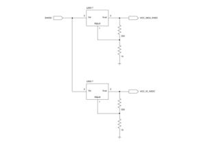
See Fig.7; because some of the MCU's digital outputs are used to directly drive LEDs or control collector/emitter current through BC547, there's quite a bit of current pulled from the MCU in total. That is why it will cause the regulator to become fairly hot.
The nice way to fix this would be to avoid driving the LEDs directly by using a transistor and using the 24VDC-rail. Instead I just put 2 regulators on there: 1 for the MCU alone, and one for the rest of IC's. I noticed that during some testing during soldering (while still components missing), some of the 74x IC's pull (much) more current when inputs are left floating. someone pointed out this is because floating hi-Z inputs pick up noise from the environment, which drives them high/low very fast; the output-side, dependent on actual gate used, thus switches continuously; this switching consumes power because of the totempole nature of the output.
Actually soldering the b*tch together
Evolution at its finest
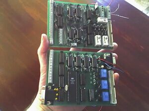
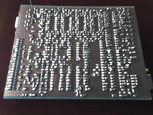
Soldering is always fun, of course; having said that, it is also very time-consuming. Described above is actually the 2nd attempt; see Fig.8 for a comparison between old (above) and new boards.
The old one cost a lot of time to make but was basically born dead because it needed too many external select- and I/O-signals. It's broken now; salvaged the relais, tossed the rest away. </whine> ;-)
Layouting vs layouting
There are a lot of wires on the board. Placing the components is a funny puzzle and fairly simple; not much to gain there when layouting properly, I guess. However, manually soldering the wires is quite a job - which would be almost solved instantlly when using a custom-made PCB instead of knaeckebr0t. Placing and soldering the components took about 1 day; my guess is that the wires took 4x that much time.
Therefore, layouting seems to get more and more interesting; perhaps next time then... The added advantage is to be able to use SMD components, finally. The added disadvantage will be having to desolder/mod them because of some bug/flaw, I guess.
Have fun -- Michai
